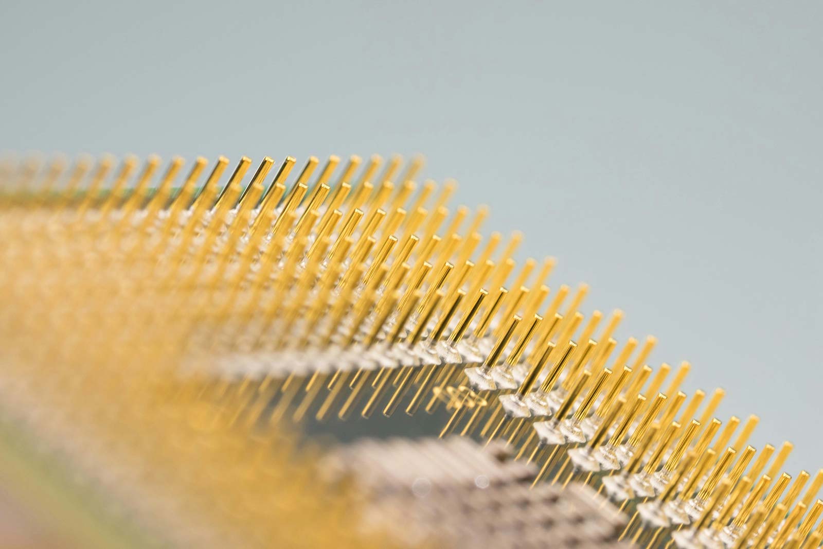
What is ENIG Plating?
Electroless Nickel and Immersion Gold (ENIG) is one of many metal plating services at Alternate Finishing. ENIG plated material has a flat, solderable surface and allows tighter placement of surface mount pads. The finish is solderable and bondable with aluminum wire.
The process line is fully automated with vibration in all process stations to ensure bubbles are removed from the holes.
Request a Quote
What ENIG Plating is Best For
Electroless Nickel Immersion Gold is a good fit when you need a flat, solder-ready surface that holds up well during storage and assembly. It’s commonly chosen for:
- Fine-pitch SMT layouts where pad flatness helps reduce defects
- BGA and dense boards where coplanarity affects yield
- Applications needing a copper diffusion barrier, since the nickel layer protects the copper
- Stable solderability over time, because the gold layer helps prevent oxidation during handling and shelf life
When repeatability matters more than anything, especially on tight features, ENIG finishing is often the safer, more consistent finish.
The ENIG Plating Process at Alternate Finishing, Inc.
Beginning with the nickel plating process, electroless Nickel (EN Plating) is applied after copper trace/feature definition (after Cu plate, image, and etch operations). During board manufacturing, it can be applied before or after the solder mask application, providing a conformal coating on all exposed copper surfaces, including sidewalls.
The deposit is a nominal 120 – 240 micro-inches of approximately 93% purity nickel over exposed copper traces and features. Intrinsic to the electroless process is a significant amount of phosphorus co-deposition with the nickel. We also have two electroless nickel choices in ENIG plating. One with 6-8% phosphorus and another with 8-10% phosphorus.
The Electroless Nickel Layer
In ENIG finishings, the electroless nickel acts as a barrier layer between the copper and the gold, preventing unwanted (non-solderable) intermetallic formation. The electroless nickel layer also adds strength to plated through holes and vias.
In the electroless nickel immersion gold process, gold is applied following electroless deposition of nickel, providing a gold coating to all exposed nickel surfaces, including sidewalls.
The Gold Layer
Gold is applied by a molecular replacement process in which previously deposited nickel molecules are replaced by gold molecules in a processing tank. In ENIG plating, pure gold is deposited that is 99.99% pure, and its thickness is typically 2 to 4 micro-inches.
By design, the immersion deposition process is self-limiting. When the underlying nickel is completely covered, the reaction will stop and no more gold will deposit. Immersion gold provides excellent solderability properties, and it retards the passivation (oxidation) of the nickel layer.
Benefits of ENIG-Finished Material
In ENIG finishing, the combined nickel/gold, or ENIG, metallization provides excellent corrosion resistance, solderability, pad coplanarity, and shelf life. Electroless Nickel and Immersion Gold is a good choice for fine-pitch SMT and BGA technologies.
Compatible Materials for ENIG Plating
Since ENIG finishing is deposited onto exposed copper, compatibility is mostly about what’s on the surface and what’s been properly removed before the finish goes on. It can be used on:
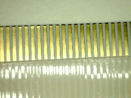
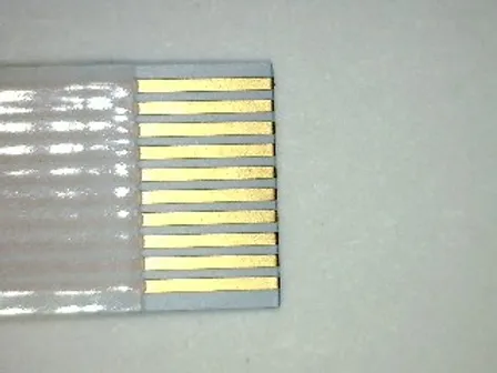
- Copper pads and traces (including fine features)
- Through-hole and via copper, where the hole walls are accessible and clean
- Boards with solder mask-defined openings, as long as the mask is fully cured and the windows are free of residue
- Bare copper panels when ENIG is applied before the solder mask, based on the build flow
- Selective areas, when ENIG plating is applied after the solder mask, only where the copper is intentionally exposed.
What usually causes problems isn’t the base material, but rather its prep: oxidation, leftover resist, contamination in pad openings, or anything that blocks the chemistry from contacting the copper evenly.
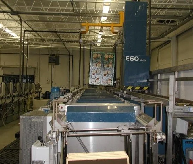
Industrial electroplating processing line with multiple tanks and an automated hoist system.
Technical Specifications and Considerations in ENIG Plating
Size limits – For electroless nickel immersion gold, the panel size most often received is 24″ x18″, but panels can be any size up to 26″ x 30″.
Alternate Finishing, Inc. can plate the whole panel after you etch it. No tin or tin lead may be exposed anywhere on the panel, including edges and inside holes.
Removing the Intermetallic Layer
During ENIG finishing, we recommend that you run the panels through the solder strip with some extra time to ensure all the intermetallic layer is removed and that you bake the panels at 250 degrees F for one hour.
For Printed Circuit Board Plating
AFI can apply ENIG plating to the pads only. This is done after you apply the solder mask on the bare copper.
If holes are plugged, they need to be completely plugged flush. Holes that are partially filled with solder mask or plugged from one side cause incomplete catalyzation, and some pads may not plate correctly.
Panels & Solder Masks
We plate panels that have many different brands of solder masks and do not recommend any particular brand or model.
However, please follow closely any recommendations that your mask supplier has regarding preparing panels for electroless nickel and immersion gold plating.
Tin & Tin-Lead
The tin or tin-lead used for etch resist must be completely removed prior to solder mask application.
Avoid tight registration of the solder mask. If possible, open a window around rows of fine-pitched features.
Solder masks must be fully cured before ENIG plating, however, take care not to over-cure them.
After Processing
Boards must stabilize after processing. Panels that fail solder mask adhesion tests after processing will likely pass in as little as a few hours or the next day. For this reason, we only tape test on waste areas of the panel for ENIG finishing adhesion tests.
What Affects Turnaround Time for ENIG Plating
ENIG turnaround time is usually driven by how ready the boards are when they arrive and how tightly the finish is being controlled. The biggest factors include:
- Incoming condition: oxidation, fingerprints, residue, and other imperfections can require extra cleaning or rework
- Resist/ mask readiness: incomplete resist removal or dirty mask openings slow processing and inspection
- Thickness targets and documentation: non-standard nickel/gold requirements, special notes, or missing specs create back-and-forth
- Panel size, rack loading, and quantity: large panels and high volume affect throughput
- Testing and inspection needs: coupons, additional verification, or reporting requirements add steps
If you send clean panels with clear requirements, ENIG plating typically moves much faster.
Advantages and Disadvantages of ENIG Plating
Electroless Nickel Immersion Gold, or ENIG, is a widely used surface finish for printed circuit boards because it combines durability with great conductivity. These factors greatly contribute to its acceptance as an industry standard used in applications ranging from consumer electronics to high-reliability sectors like aerospace and medical devices.
The plating process has many technical benefits that make it a favorable option for creating solderable surfaces on PCBs and other electronic components, but it also has disadvantages that make other plating options more favorable. Here is a comparison of both.
| Advantages | Disadvantages |
|---|---|
| Flat Surface: ENIG plating results in a highly flat surface, ideal for fine-pitch components and complex PCB designs | Higher Cost: ENIG finishing is more expensive compared to other PCB finishes like HASL (Hot Air Solder Leveling). |
| Excellent Solderability: The gold layer formed after the gold deposition offers excellent solderability, preventing oxidation and ensuring a longer shelf life. | Black Pad Defect: Improper process control can lead to “black pad,” a defect where the nickel corrodes, weakening solder joints. |
| Durability: The nickel layer is robust, providing wear resistance and protection from environmental factors. | Complex Process: The multi-step chemical process is more complex and requires careful monitoring, increasing production time and costs. |
| RoHS Compliance: Electroless Nickel Immersion Gold is a lead-free surface finish, meeting environmental regulations like RoHS (Restriction of Hazardous Substances). | Nickel Corrosion: The nickel layer, if not properly handled, can corrode, affecting the performance of the board. |
| Long Shelf Life: Due to the gold finish, ENIG can maintain solderability over a longer period compared to other finish options. | Longer Production Time: Due to the multiple layers and stringent quality control required for ENIG plating, timely completion is a challenge. It typically takes longer to manufacture compared to simpler finishes like OSP (Organic Solderability Preservatives). |
Industries We Serve
ENIG serves a vital role for many of the industries we serve. Here are just some the applications:
High-Tech Industry
In high-tech metal plating, we focus on precision, reliability, and optimal performance at Alternate Finishing, Inc. Here are some advanced plating solutions we use in different applications.
- Semiconductor Manufacturing: We provide electroless nickel immersion gold services for semiconductor components, ensuring excellent solderability and corrosion resistance. Our processes support fine-pitch components and complex PCB plating designs that are used in modern electronic devices.
- Telecommunications: For high-frequency applications, our plating services enhance signal integrity and reduce loss. The flat, uniform surface achieved through ENIG plating is perfect for high-speed data transmission equipment.
- Consumer Electronics: For consumer electronics, we focus on durability and reliable performance of the products. We achieve this by providing plating solutions like ENIG finishing, which are resistant to wear.
Healthcare
Medical PCB finishing services require the highest standards of quality and biocompatibility and AFI provides the plating solutions needed to meet these requirements.
- Medical Imaging Equipment: We offer plating solutions that enhance the conductivity and reliability of components used in MRI, CT, and X-ray machines. Our finishes ensure a stable performance over the equipment’s lifespan.
- Diagnostic Instruments: Diagnostic tools must be precise. Our ENIG plating provides a uniform, corrosion-resistant surface that is needed for accuracy in readings and long-term reliability.
- Implantable Devices: These devices must be biocompatible and durable. We follow stringent medical standards in our plating processes to provide safe and reliable finishes on components used in these devices.
Military, Aerospace, and Automotive
The components used in these industries must be capable of performing reliably in extreme conditions like high and varying temperature ranges. At AFI, our metal plating services meet these rigorous standards with our electroless nickel immersion gold techniques. We offer ITAR-registered metal finishing services for defense-related projects..
- Avionics Systems: Our efficient ENIG plating ensures excellent solderability and corrosion resistance for avionics PCBs, critical for flight control and navigation systems.
- Defense Electronics: We provide durable plating solutions like ENIG finishing for military communication devices, radar systems, and other defense electronics, ensuring the reliability of military PCBs in harsh environments.
- Satellite Technology: In space applications, components must endure extreme temperatures and radiation. Our plating services offer the necessary protection and performance for satellite electronics.
- Engine Control Units (ECUs): Our plating technology solutions ensure the reliability and durability of ECUs, which are critical for vehicle performance and efficiency.
- Infotainment Systems: We provide ENIG plating services for components used in automotive infotainment systems, ensuring excellent signal integrity and durability.
- Safety Systems: For safety-critical components like airbag controllers and anti-lock braking systems, our plating processes provide the necessary reliability and performance.
Common Part Types We Plate with ENIG Plating
ENIG plating at Alternate Finishing, Inc. is most commonly applied to printed circuit boards and electronic components where the finish has to be uniform across real-world features, not just flat test coupons. That typically includes:
Board formats we see often:
- Rigid, flex, and rigid-flex circuits, including larger panels (up to 26” x 30”)
Features ENIG is used for:
- Exposed copper pads and contact areas that need a consistent, solderable surface
- Holes and vias (including tight geometries) where conformal coverage matters
- Fine features where uneven finishing becomes an assembly risk
Work With Us
At Alternate Finishing, Inc., we can help you meet your ENIG finishing needs. While we have a fast service with quick turnarounds, we also always deliver highly reliable finishes. Request a quote.
Frequently Asked Questions
What makes ENIG plating different from other PCB surface finishes like HASL or OSP?
Electroless nickel immersion gold provides a flat, solderable, and corrosion-resistant surface, making it ideal for fine-pitch SMT and BGA components. In contrast, HASL is less planar and OSP offers shorter shelf life and oxidation protection.
What thicknesses of nickel and gold are used in ENIG finishing?
At Alternative Finishing, Inc., we base these ENIG plating thicknesses on IPC-4552 standards. This means around 100–250 µin (≈2.5–6 µm) for Nickel and 2–8 µin (≈0.05–0.2 µm) for immersion gold.
What causes the “black pad” defect, and how can it be prevented?
“Black pad” occurs from excessive phosphorus corrosion of nickel during gold immersion. To avoid it, you must have strict control of Ni-P chemistry and gold immersion timing. Our recommendation? Let our professionals help you achieve that.
Can ENIG-coated boards be wire-bonded with gold or aluminum wire?
Yes, ENIG supports aluminum wire bonding thanks to its flat, Au-covered surface. For gold wire bonding, a thicker 10–25 µin “soft gold” top layer is needed, and this is often achieved via additional electroless or electrolytic gold.
What factors influence the cost and turnaround time of ENIG plating?
This process involves multiple chemical steps and gold usage, which makes it more costly and time-consuming than finishes like HASL or OSP. Costs depend on panel size, gold thickness, and plating precision.
Is ENIG suitable for high-reliability industries?
Yes. It offers long shelf life, EMI protection, and the performance needed for aerospace, medical, telecommunication, defense, and other applications where high reliability is important.