The Rundown
- ENIG PCB uses nickel and gold layers for flat, oxidation-resistant surfaces.
- It offers excellent solderability, corrosion protection, and wire bonding.
- Common in high-reliability, fine-pitch, and consumer electronics.
- Costs more than HASL/OSP, but quality checks (XRF, solderability tests) ensure consistency.
What is ENIG PCB Finishing?
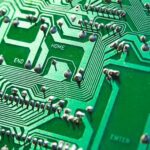
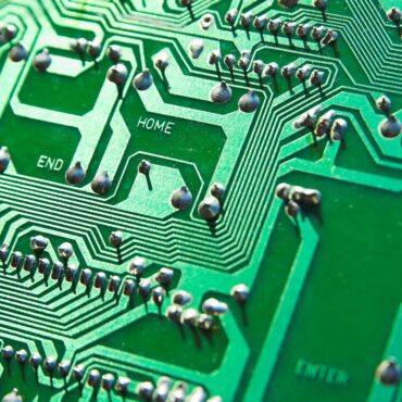
The ENIG surface finish is a two-step metal coating applied to exposed copper pads on a printed circuit board. The reason we use it a lot is because it stays flat, resists oxidation in storage, solders predictably on tiny pads and dense components, and so on, as we will discuss later on.
A Brief Explanation of the ENIG Process
Here is how we do it at Alternate Finishing, Inc.:
- We begin by cleaning and activating an etched board.
- We then use an electroless (no external power) nickel bath to chemically deposit a uniform nickel layer onto the copper.
- In a second bath, immersion gold “displaces” a very thin layer of gold onto that nickel.
The ENIG PCB chemistry makes the finish even across the panel and inside tight features, which is great for fine-pitch assembly.
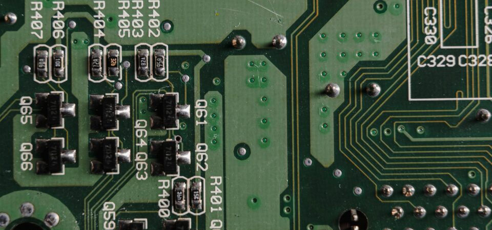
Layers Involved
- Copper: This is the base circuitry that we need to protect until soldering.
- Nickel (electroless): A hard diffusion barrier that provides the real solder joint interface and maintains flatness/coplanarity.
- Gold (immersion): This is a very thin, protective top layer that keeps the nickel from oxidizing during storage and handling. It dissolves into the solder during reflow.
The Benefits of ENIG Surface Finish
- Excellent solderability: With ENIG PCB finishing comes great solderability because of the flat and uniform surface it creates. This is useful for applications where even slight irregularities can cause defects.
- Corrosion resistance: The thin gold layer acts as a protective shield over the nickel barrier to keep oxidation away during storage and handling. This ensures that boards remain solderable even after longer shelf lives or transport across varied environments.
- Good wire bonding performance: The nickel barrier layer provides a stable base, while the immersion gold allows reliable wire bonding with gold or aluminium wires in specialized assemblies.
- Flat surface for surface mount technology (SMT): A major advantage of ENIG PCB finishing is planarity. Again, thanks to the smooth, level finishing, stencil printing, and component placement during the SMT process is simplified. This reduces defects and rework, too.
- Lead-free compliance: ENIG is fully compatible with RoHS requirements and other global lead-free standards, making it a safe choice for manufacturers navigating today’s compliance landscape.
Applications of ENIG Surface Finish

High-reliability electronics
Think about pcb plating for medical devices, aerospace modules, or defense systems. These are places where a circuit board simply can’t fail.
Engineers often choose ENIG for PCBs because the finish holds up against corrosion and creates dependable solder joints that won’t degrade quickly.
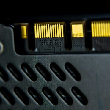
Fine-pitch devices
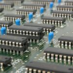
As component sizes shrink, you don’t have much room for error. Ball grid arrays, QFNs, and other dense packages need a surface that’s perfectly flat so solder paste spreads evenly and parts actually seat the way they’re supposed to.
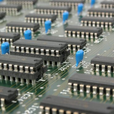
Consumer electronics
On the other end of the spectrum, ENIG shows up in everyday items like phones and tablets. These products pack a lot into very small boards, and manufacturers don’t have time for soldering surprises.
When Long-Term Reliability Matters
Some boards sit on the shelf before they’re used; others operate in the field for many years without much servicing. In both cases, you need a surface finish that still solders cleanly when the time comes.
Potential Drawbacks of ENIG PCB Finishing and The Solutions
- The ENIG surface finish isn’t the cheapest finish. In fact, its process makes it pricier than HASL or OSP.
- Another concern is the “black pad” defect, where the nickel layer turns brittle and causes joint failures. But this is prevented by careful bath control and inspection.
Quality Considerations
Nickel is typically 3 to 6 microns thick, with a very thin gold layer on top. Shops confirm this using XRF and solderability testing, sometimes backed by cross-sections to keep the finish reliable and consistent.
Work With Us
ENIG PCB is a strong default for fine-pitch high-reliability builds. Work with Alternate Finishing, Inc. for a reliable finish.
We can also help you review designs and share data. See our ENIG overview and ITAR-registered services to turn an ENIG surface finish into real assembly insurance. Request a quote.

Robert Peterson is President of Alternate Finishing, an AS9100D, ISO 9001:2015, and ITAR registered metal finishing provider serving customers across the USA and Canada. With more than four decades of experience in printed circuit boards and metal finishing, Robert is certified by the National Association of Metal Finishers as an electronic specialist. He’s also an avid photographer.